

Every engineer who has debugged a failed prototype has had the same thought at some point during the process: 'I should have simulated this.' The voltage reference that drifted out of tolerance. The regulator that overheated under load. The bias network that shifted just enough to push a downstream stage out of its operating window. These are problems that simulation can catch definitively, well before a board is fabricated. The mathematics are straightforward. The tools exist. The component data is available.
And yet, in the vast majority of PCB design projects, the circuits that fail on the bench were never simulated at all.
This is not because engineers are unaware of simulation's value. It is because the practical realities of simulation, as it exists today, make comprehensive coverage effectively impossible under real project constraints. The result is a persistent gap between what behavioral verification could catch and what it actually catches: a gap that compounds with every other validation weakness to produce the stubborn respin rates the industry has come to accept as normal.
The first article in this series identified two compounding gaps in schematic-level validation: spec compatibility checking and behavioral verification [1]. This article examines the second gap in full. Why do the simulation tools that exist -- tools that are technically capable of answering critical design questions — fail to provide systematic verification coverage for real-world projects? And what would it take to close that gap?
What simulation can reveal
Circuit simulation, particularly SPICE-based analysis that has been the industry standard since its development at UC Berkeley in the 1970s [2], can answer precise questions about circuit behavior that no amount of datasheet cross-referencing can address. A DC operating point analysis computes the actual voltages and currents at every node in a circuit for a given set of conditions. Tolerance analysis reveals how circuit performance shifts when component values drift across their specified ranges. Power dissipation calculations determine whether a device is operating within its thermal limits given the specific voltages and currents of a particular design, not just the rated maximums on a datasheet.
Consider a bias resistor network setting the feedback ratio on a precision voltage reference. The nominal output voltage is correct, and both resistors pass every specification check: voltage rating, power dissipation, tolerance grade. But this particular design uses 1% resistors from the E96 series [3], and the downstream ADC has a reference input window of only 30 mV. When both resistors drift to opposite ends of their 1% tolerance bands simultaneously, the reference output shifts by 45 mV, outside the acceptable window. No specification is violated. Both components are operating within their rated parameters. But the circuit does not deliver an acceptable output under worst-case conditions, and only a simulation that sweeps the tolerance range can reveal where the margin disappears.
Or consider a linear regulator stepping 12V down to 3.3V for a sensor subsystem drawing 250 mA. Every datasheet specification checks out: the input voltage is within range, the output current is well under the rated maximum, and the dropout voltage is satisfied. But the actual power dissipation in this specific application is (12V - 3.3V) x 0.25A = 2.175W [4]. In a small SOT-223 package with limited copper area, that puts the junction temperature within a few degrees of the thermal shutdown threshold at the high end of the operating temperature range. The datasheet contains every number needed to calculate this, but the answer depends on the specific operating point of the regulator in this particular circuit. An engineer who checks only that the load current is 'within the rated capacity' misses the thermal problem entirely.
These are not exotic analyses. They represent the most fundamental level of behavioral verification: confirming that the circuit operates as intended at its DC operating point, across the range of component values and conditions it will encounter. The tools to perform them have existed for decades and are well understood by the engineering community [5]. The question is not whether simulation works. The question is why it so rarely gets applied comprehensively.

The five barriers to simulation at scale
The gap between simulation's capability and its actual deployment in PCB design projects is not a single problem. It is the compounding effect of five distinct barriers, each of which individually discourages comprehensive simulation and together make it practically impossible under typical project constraints.
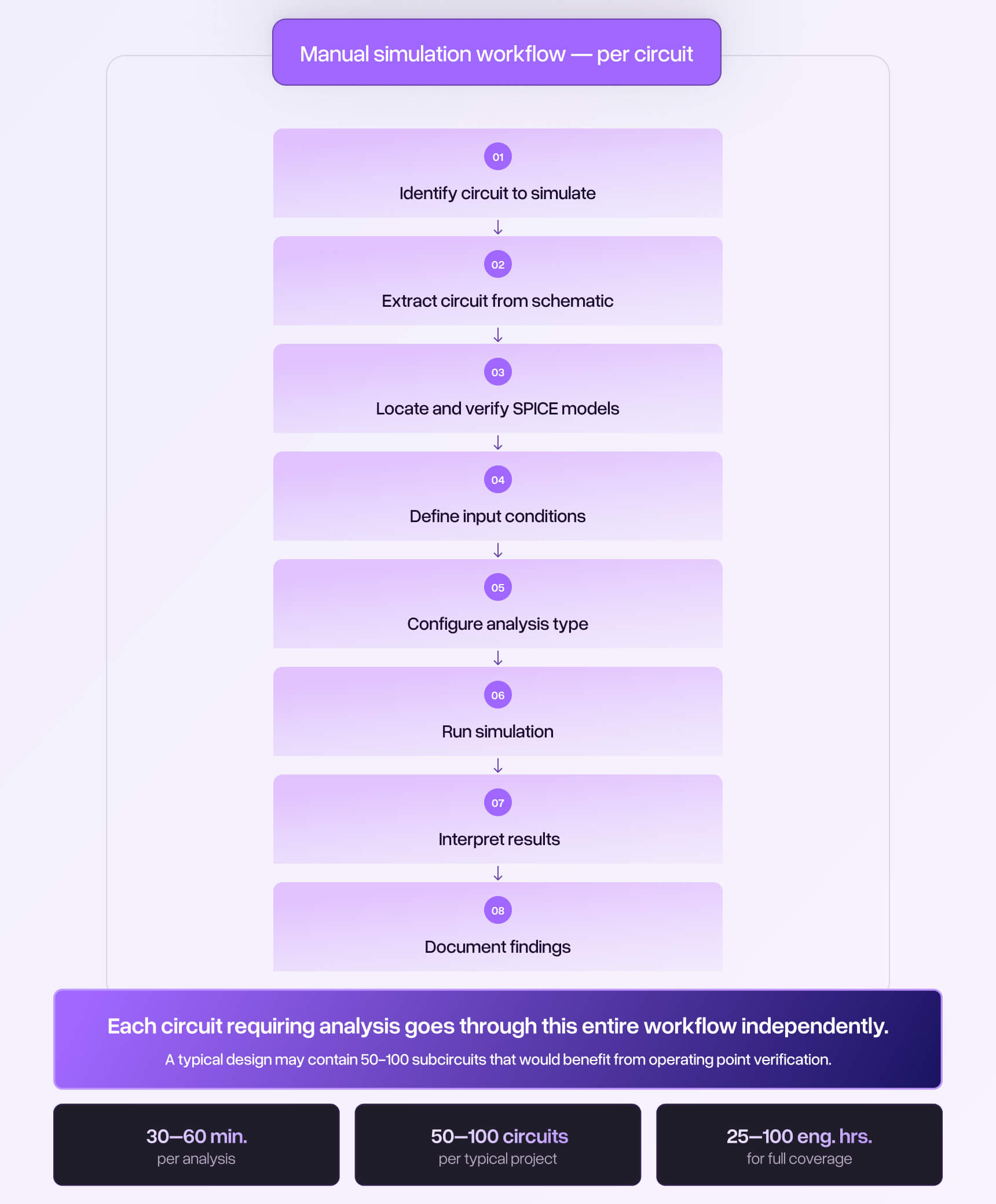
The manual setup burden
Every simulation requires explicit, manual configuration. There is no 'simulate everything' button. For each analysis, an engineer must isolate the circuit of interest from the larger schematic, define the input conditions and stimulus, select or verify appropriate component models, configure the analysis type and parameters, run the simulation, and interpret the results in the context of the design intent.
For a single analysis, this process might take thirty minutes to an hour, depending on complexity. For a straightforward tolerance check on a resistor network, it might take fifteen minutes if the models are readily available. But a moderately complex PCB design might contain dozens of subcircuits that would benefit from operating point verification: voltage references, bias networks, power regulation stages, sensor interface circuits, signal conditioning chains, and protection circuits. Performing even basic DC operating point analysis on every circuit that warrants it could require dozens of individual simulation setups.
Under real project timelines, this is simply not feasible. Engineers must triage. They simulate the circuits they judge to be most critical or most uncertain, and they leave the rest to manual review, engineering judgment, or hope [6]. The decision about what to simulate and what to skip is itself an exercise in risk assessment that receives little formal attention in most design processes.
The expertise requirement
Setting up a simulation correctly requires more than knowing how to use the tool. It requires understanding what questions to ask, how to frame those questions as simulation configurations, and how to interpret the results in context.
Model selection is a particular challenge. SPICE models vary significantly in quality and applicability. Not all models are created by the component manufacturer, and even manufacturer-provided models may not accurately represent behavior at the operating conditions relevant to a particular design. As one industry analysis noted, the quality of SPICE models can vary significantly, and using a model inappropriately can lead to inaccurate results or simulation errors [7]. For components where no manufacturer model exists, an engineer must either build a custom model from datasheet parameters, use a generic approximation, or forgo simulation of that circuit entirely.
Boundary condition definition presents a similar challenge. The results of a simulation are only as good as the conditions applied to it. If the input voltage range is defined too narrowly, or the load current profile does not reflect actual operating conditions, or the temperature range does not span the intended deployment environment, the simulation may produce reassuring results that do not reflect reality. Setting up boundary conditions correctly requires understanding not just the circuit under test but its context within the larger system.
Results interpretation adds another layer. A simulation that converges and produces numbers is not the same as a simulation that answers the right question. An engineer must understand what the numbers mean in context, where the margins are, and what happens when conditions change. This interpretive step is where experience matters most, and it is not something that can be easily systematized or delegated.
The subsection limitation
Current simulation tools analyze circuits in isolation. An engineer extracts a portion of the schematic, defines its boundaries, applies stimulus, and observes the response. This approach works well for individual subcircuits but fundamentally cannot capture interactions between subsections of a larger design.
In a real PCB, circuits do not operate in isolation. The output of one stage feeds the input of another. Power supply rails are shared across multiple loads, and the behavior of one load affects the voltage available to others. A voltage reference that performs perfectly when simulated with an ideal load may behave differently when its output is loaded by the actual combination of circuits it feeds in the real design.
Simulating the entire design as a single analysis is theoretically possible but practically infeasible for most board-level designs. The complexity of managing hundreds or thousands of component models, defining appropriate stimulus for every input, and interpreting a full-board result set exceeds what most engineers have the time or motivation to attempt, even when the tools technically permit it [8]. The result is that simulation provides a series of isolated snapshots rather than a comprehensive picture of system behavior.
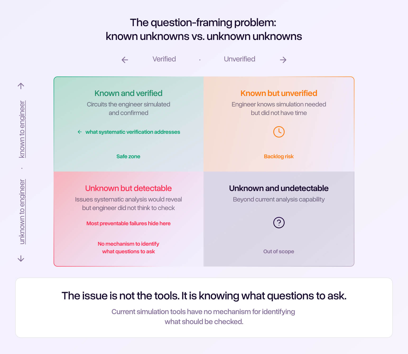
The question-framing problem
This may be the most fundamental barrier of all. Simulation tools only answer questions the engineer thinks to ask.
If the engineer does not think to check the power dissipation in a particular regulator, that analysis does not happen. If the engineer does not consider the worst-case tolerance stack in a particular reference network, that risk goes unquantified. If the engineer assumes a bias network is well within its operating range and does not simulate it, a marginal condition that would have been immediately obvious in a simulation result goes undetected until the bench.
This is the 'unknown unknowns' problem applied to circuit verification. The circuits that get simulated are the ones the engineer already suspects might be problematic -- the ones where risk is apparent. The circuits that do not get simulated are the ones that look routine, the ones where the engineer's mental model says 'that should be fine.' But engineering experience teaches a painful lesson: the circuits that cause bench surprises are disproportionately the ones nobody thought to question [9].
No amount of simulation capability can compensate for a question that is never asked. This is a structural limitation of the current simulation paradigm, not a limitation of the tools themselves.
The time and resource constraint
Even an engineer who is willing to simulate comprehensively, who has the expertise to set up analyses correctly, who understands the question-framing challenge, and who has access to appropriate models for every component, faces a simple arithmetic problem: there is not enough time.
A moderately complex industrial design might contain fifty to a hundred distinct subcircuits that could benefit from at least basic operating point verification. If each simulation setup takes an average of thirty minutes, including model verification, configuration, execution, and results interpretation, comprehensive coverage would require twenty-five to fifty engineering hours. That is a full week of a senior engineer's time, devoted entirely to simulation setup and analysis, on a single project.
In an environment where that same engineer is likely juggling two or three concurrent projects, managing component sourcing issues, responding to layout questions, attending design reviews, and facing a fabrication deadline, allocating a full week exclusively to simulation is a budget decision that most project schedules simply cannot accommodate [10]. The result is predictable and consistent across the industry. Engineers simulate a handful of circuits they judge to be most critical, and they accept the residual risk on everything else.
The coverage gap in practice
The compounding effect of these five barriers produces a predictable coverage pattern across the industry: most circuits in a typical design never get simulated at all.
Published data on what fraction of a typical PCB design actually receives simulation coverage is scarce, because most organizations do not track this metric. But the pattern is consistent enough in industry practice to describe with confidence: engineers simulate the circuits they are least confident about. A new power supply topology, an unfamiliar sensor interface, a circuit operating near the limits of component ratings. These get simulated because the risk is visible and the engineer feels uncertain.
What does not get simulated is everything that looks routine. The resistor divider with standard 1% components. The linear regulator that has been used in a dozen previous designs. The bias network that 'obviously' works because the nominal values check out. The protection circuit that mirrors a reference design. These circuits are assumed to be correct because they are familiar, and familiarity breeds confidence.
But familiarity is not verification. A regulator that worked in a previous design at 5V input may quietly exceed its thermal limits when reused at 12V input with a higher load. A voltage divider that worked with 5% resistors may not maintain adequate margin when the downstream component's input window tightens on a new revision. The assumption that 'it worked before' substitutes history for analysis.
The result is a pattern that engineers recognize but rarely quantify: the circuits that fail on the bench are often the ones nobody thought to simulate. The thermal problem in the 'proven' regulator. The tolerance stack in the 'standard' voltage reference. The bias point drift in the 'routine' sensor interface.

The garbage-in problem
There is a further complication that does not receive enough attention: simulation that is performed but configured incorrectly can be worse than no simulation at all.
An engineer who skips simulation and relies on manual review at least knows they are accepting risk. An engineer who runs a flawed simulation and receives reassuring results believes the risk has been retired. The latter is more, not less, likely to be surprised on the bench.
A simulation that produces results, even incorrect ones, generates confidence. The engineer sees numbers, compares them against expected values, and concludes the circuit is validated. But if the component models do not accurately represent the devices being used, or if the boundary conditions do not reflect the actual operating environment, or if the analysis type does not capture the failure mode that will manifest on the bench, the simulation provides false assurance rather than genuine validation.
SPICE model quality is a well-known challenge in the simulation community. Component manufacturers provide models of varying fidelity, and not all components have manufacturer-provided models at all [12]. For components that do have models, the model may have been developed for a different operating regime, may use simplifications that are inappropriate for the current application, or may simply be outdated relative to the current production silicon. One analysis of the MOSFET modeling landscape found that some manufacturer-supplied models still use outdated Level 1 through Level 3 formulations that can exhibit non-physical behavior and convergence problems, despite decades of improvements in modeling methodology [13].
This creates a particularly insidious failure mode. False confidence from a flawed simulation is harder to debug than the honest uncertainty of not having simulated at all, because the engineer has already 'checked' and moved on.
What closing this gap would require
Understanding the barriers makes it possible to describe the shape of a solution, even without reference to any specific product or approach.
The essential insight is that the five barriers are interconnected. A partial solution that addresses one or two while leaving the others intact will produce only marginal improvement. Automating simulation setup does not help if the engineer still has to identify which circuits need analysis. Providing better models does not help if project timelines still prevent comprehensive coverage. Each barrier reinforces the others.
What the industry needs is a fundamental shift in how behavioral verification is conceived: from a specialized activity performed by an expert on selected circuits, to a systematic process applied to the design as a whole. The intelligence required is not primarily computational. It is the ability to examine a circuit, understand what it is supposed to do, determine what questions need to be answered, and evaluate the results against the design's actual requirements. This is, in essence, what an experienced senior engineer does when reviewing a colleague's work. The challenge is that this process does not scale when it depends entirely on the time and attention of human experts.
It is worth noting that the need for systematic behavioral verification extends well beyond the DC operating point domain discussed in this article. Transient behavior, AC performance, stability analysis, and other dynamic characteristics are equally important for many circuits. But even restricting the scope to the most fundamental level of verification -- DC operating point analysis across component tolerance ranges — the gap between what should be checked and what actually gets checked is substantial.
The engineers who build complex PCBs today are not lacking in skill, tools, or knowledge. They are lacking in a mechanism that brings the right analysis to bear on the right circuit at the right time, comprehensively across the design, without requiring the engineer to identify every question individually. Until that mechanism exists, the behavioral verification gap will continue to drive a predictable and persistent fraction of the industry's most expensive and preventable prototype failures.
![Side-by-side timeline comparison. Left column: 'Software QA Evolution' showing progression from Manual Code Review (1990s) to Automated Unit Testing (2000s) to Continuous Integration/CD (2010s) to AI-Assisted Quality Assurance (2020s). Right column: 'Hardware Design Validation' showing progression from Manual Peer Review (1990s) to Design Rule Checking (2000s) to Simulation Tools -- manual, sporadic, subsection-limited (2010s) to [gap marked with '?'] (2020s). Annotation: 'The systematic, integrated verification layer is still missing.'](https://cdn.prod.website-files.com/698fa432fdb18648b96819b9/69e626d676af909741058f3e_visual%207.jpg)
References
- 'The Hidden Cost of PCB Respins: Why 90% of First Prototypes Fail,' Cadstrom Blog, Article 1 of 5.
- Nagel, L.W. and Pederson, D.O. (1973). 'SPICE (Simulation Program with Integrated Circuit Emphasis).' University of California, Berkeley. First presented at the 16th Midwest Symposium on Circuit Theory, 1973.
- IEC 60063, 'Preferred Number Series for Resistors and Capacitors.' International Electrotechnical Commission. Defines standard tolerance series for passive components, including the E96 (1%) and E24 (5%) series.
- Texas Instruments, 'Understanding Linear Regulator Thermal Considerations,' Application Report SLVA118A, April 2003, revised June 2008. Documents the calculation of power dissipation as P = (V_in - V_out) x I_load.
- 'What is SPICE Simulation?' Cadence Design Systems. Notes that 'SPICE simulation has been an industry staple for decades.'
- 'Five Reasons to Use SPICE Simulation,' EMA Design Automation, January 2024.
- 'SPICE Simulation Overview,' National Instruments. Notes that 'the quality of SPICE models can vary, and not all SPICE models are applicable to every application.'
- 'Modeling for Printed-Circuit Board Simulation,' IEEE Spectrum. Identifies the 'lack of appropriate models for some of the components used in PCB designs' as a serious practical barrier.
- 'Modern Practices in PCB Design Verification,' Design World Online, citing Lifecycle Insights research, September 2018.
- 'How to Reduce Respins of Your PCB Using SPICE Simulation,' Cadence PCB Design Blog, 2019.
- 'The New Shift-Left Multi-Dimensional PCB Design-Verification Platform,' Electronic Design, citing Lifecycle Insights. Reports that '58% of all new product design projects incur added costs and time delays.'
- 'SPICE vs. IBIS: Choosing the More Appropriate Model for Your Circuit Simulation,' Analog Devices.
- Elder, S. 'Pick Your SPICE Models Carefully,' Planet Analog, April 2013.