'The Validation Gap'
/
Part
1
of
5


There is a moment every hardware engineer knows. The prototype boards have arrived from fabrication. Assembly is complete. You connect the power supply, double-check the voltage, and flip the switch.
Sometimes there is smoke. Sometimes there is silence where there should be data. Sometimes everything appears to power up correctly, but the communication bus is dead, or a sensor returns garbage, or a peripheral simply refuses to initialize. And then begins the slow, sinking process of working backward through the schematic, searching for the mistake you already know is there, because you have been through this before.
This is not a story about one unlucky project or one careless engineer. Industry data paints a picture that should concern every hardware organization: approximately 90% of PCB prototypes fail to meet their functional, manufacturability, or scalability goals on the first attempt, forcing redesign iterations, timeline delays of four to eight weeks, and costs of $3,000 to $15,000 per failed attempt [1]. That figure encompasses the full spectrum of prototype failures, from manufacturing defects to incomplete testing to design errors. But within that broad landscape of failure, a disproportionate share of the most expensive and preventable problems trace back to a single domain: errors in the schematic that no amount of physical inspection or manufacturing optimization can fix.
This article examines why PCB respins remain so persistent, where the most damaging errors actually originate, and why the tools and processes most teams rely on leave a critical gap in design validation.
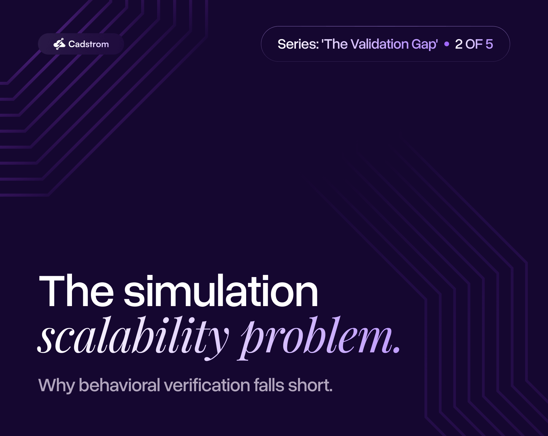
The scale of the respin problem is well documented, even if it is rarely discussed openly. Research from Lifecycle Insights found that the typical PCB project goes through 2.9 respins, with an average schedule impact of 8.5 days and a cost of $44,000 per respin [2]. For high-performance designs, those costs are often significantly higher.
Consider what that means for a mid-sized engineering team running six to eight projects per year. At 2.9 respins per project and $44,000 per respin, a team can easily accumulate $500,000 to $1 million annually in respin-related costs alone. That figure does not include the engineering hours spent debugging, the opportunity cost of delayed product launches, or the downstream effects on firmware development, integration testing, and regulatory certification timelines.
The remarkable thing about these numbers is how widely they are accepted as normal. As one industry analysis noted, many companies 'agree that three or more respins of a PCB is the natural order of the universe' [3]. Three respins is not treated as a process failure. It is treated as an inevitability, baked into project schedules and budgets as though it were a law of physics rather than a symptom of inadequate validation.
But these are not random manufacturing defects or unpredictable component failures. The vast majority of respins stem from errors that were present in the design before fabrication files were ever generated. Industry estimates suggest that a very large percentage of preventable respins originate from functional errors in the schematic domain: mistakes in how components are connected, configured, and specified that have nothing to do with physical layout or manufacturing processes [4]. These are the errors that survive every DRC check, pass every visual inspection, and reveal themselves only when the board is powered up and something does not work.
To understand why respin rates remain stubbornly high despite decades of improvement in EDA tooling, it helps to distinguish between two fundamentally different categories of design error.
Layout and manufacturing errors involve the physical realization of a design: trace widths and spacing, impedance control, thermal relief, copper pour geometry, solder mask clearance, and the many constraints that determine whether a design can be reliably fabricated and assembled. These are the errors that Design for Manufacturability (DFM) reviews and layout-focused design rule checks are built to catch. Significant progress has been made in this domain, with modern EDA tools providing increasingly sophisticated layout validation.
Schematic-level functional errors are a different animal entirely. These are errors in the logical design itself: the way components are interconnected, the compatibility of voltage domains across interfaces, the correctness of communication bus wiring, the adequacy of component ratings for the operating conditions, the polarity of signals and components, and the assignment of microcontroller peripherals to physical pins. These errors live in the schematic, not the layout. They determine whether the circuit will actually function as intended, regardless of how perfectly it is manufactured.
The critical distinction is this: a board can be flawlessly manufactured from a flawed schematic, and it will fail every time.
Schematic-level errors are particularly expensive because of when they are discovered. Layout and DFM problems are often caught during fabrication or assembly review. Schematic errors, by contrast, typically survive all the way through manufacturing and reveal themselves only during prototype bring-up or functional testing. By that point, the cost of the fabrication run, the component procurement, and the assembly are already sunk. The debugging process that follows is often the most expensive part, as engineers work backward from symptoms that may be subtle and misleading.

The schematic validation problem is actually two problems stacked on top of each other, and their effects compound.
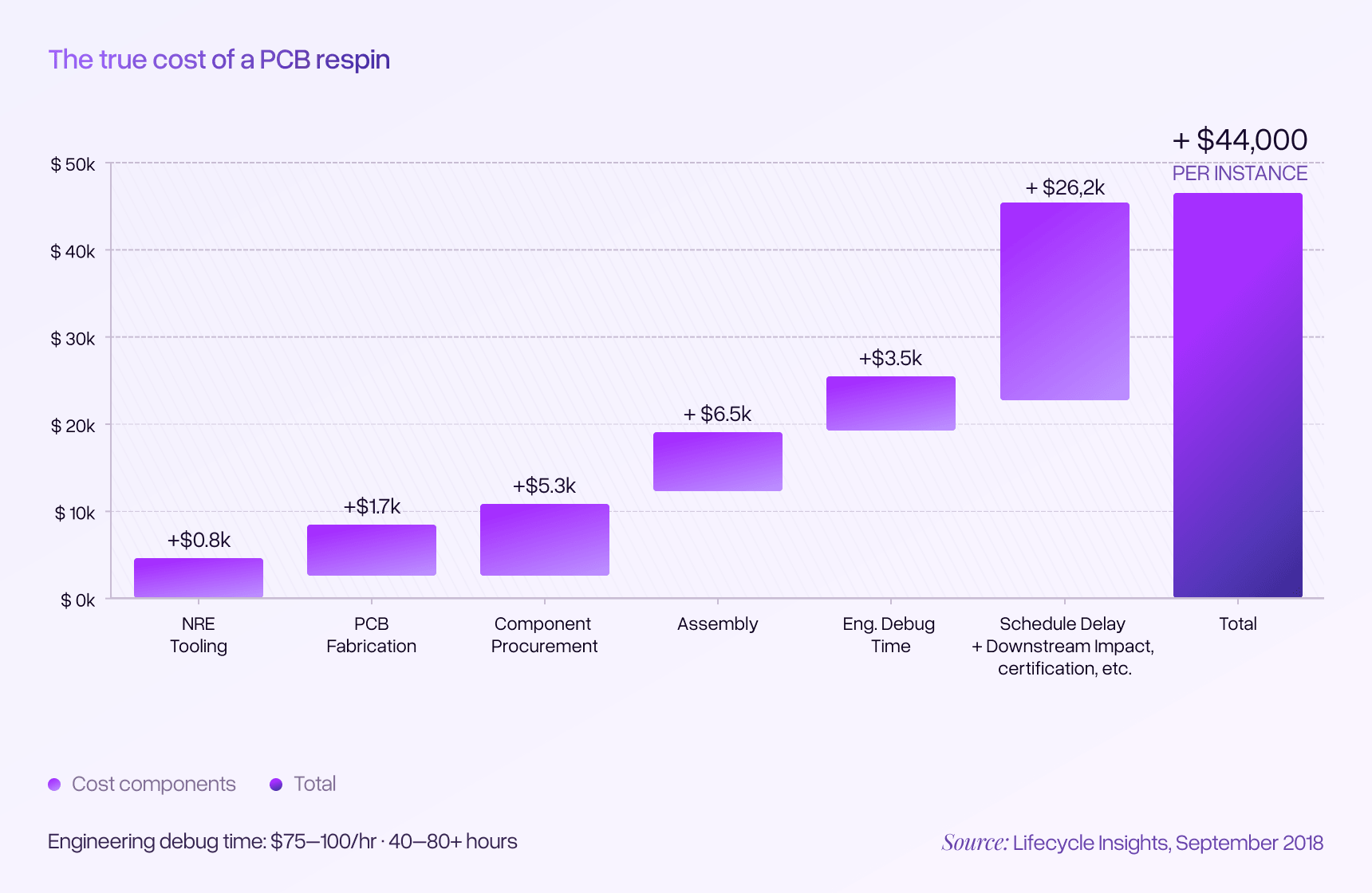
The first layer — verifying that component specifications are compatible across the design — is the one most engineers think of when they hear 'design validation.' No standard EDA tool performs this cross-referencing automatically. DRC checks physical rules, not functional ones. The work falls entirely to the engineer, who must manually verify hundreds of connections against dozens of datasheets.
Research on complex inspection tasks has consistently shown that this kind of work exhibits error rates of 20% to 30%, even among experienced professionals [5]. Those error rates are not a reflection of engineering competence. They are a reflection of cognitive reality.
Engineers working on complex designs are rarely reviewing a single schematic in isolation. They are juggling multiple projects, responding to urgent requests, making component substitution decisions, and managing schedule pressure. Context switching between these demands degrades the sustained, focused attention that thorough verification requires. When you are verifying your two hundredth pin connection of the day while simultaneously tracking a component sourcing crisis on another project, your brain begins to skim rather than scrutinize. This is not carelessness. It is the predictable consequence of asking human cognition to perform a task it is not well suited for under conditions that make it even harder.
There is also the problem of familiarity blindness. The engineer who created a schematic has spent hours or days building it, and their brain has already formed a model of what the design is supposed to do. When they review their own work, their perception is shaped by their intent. They see what they meant to draw, not necessarily what they actually drew. Peer review helps, but peers are also busy, may lack the full context of design decisions, and face the same cognitive limitations under the same time pressure.
The result: some fraction of spec incompatibilities will always escape manual review. That fraction translates directly into respins.
But spec compatibility is only part of the picture. Even when every individual component is correctly specified and every connection is compatible on paper, circuit behavior emerges from the interaction of multiple elements. Understanding whether a circuit will actually work as intended requires more than checking specifications against one another. It requires understanding what the circuit is doing: how the capabilities and performance boundaries of the components manifest as actual circuit behavior.
Consider a simple voltage divider feeding a reference input. Both resistors are within their power ratings. The nominal output voltage is correct. Everything looks fine on the schematic. But what happens when both resistors sit at opposite ends of their tolerance ranges? Does the output still fall within the required window for the downstream component? A datasheet cross-check confirms the resistors are rated appropriately, but only an operating point analysis across the tolerance range can confirm the divider actually delivers an acceptable voltage under worst-case conditions.
Or consider a linear voltage regulator providing power to a sensitive analog circuit. The regulator's output voltage is nominally correct. The load current is within the regulator's rated capacity. But what is the actual power dissipation in the regulator given the specific input voltage and load current of this design? Is the regulator operating within its safe thermal limits, or is it quietly approaching a boundary that will cause shutdown or degraded performance? The datasheet contains the information needed to answer this question, but the answer depends on the specific operating point of the regulator in this particular circuit — something that requires calculation or simulation rather than a simple spec comparison.
These questions live in the domain of simulation. DC operating point analysis can answer them definitively, exercising the design against the actual limits of its components to find where behavior meets intent and where it diverges.
The tools to perform these simulations exist, of course. But in practice, today's simulation environments are intensively manual to configure, require significant expertise to set up correctly, and are prone to producing misleading results when models or boundary conditions are configured improperly. They can only examine isolated subsections of a complex design, leaving the interpretation of results in the larger context up to the individual engineer. Most critically, simulation tools only answer the specific questions an engineer thinks to ask. If the engineer does not think to check the power dissipation in a particular regulator, or the worst-case tolerance stack of a particular voltage divider, that analysis simply does not happen.
There is also the problem of scale. A moderately complex design might contain dozens of voltage references, bias networks, power domains, and interface circuits, each of which could benefit from operating point verification. Doing this comprehensively would require setting up and running scores of individual analyses. Under real project constraints, engineers can only simulate a handful of circuits they judge to be most critical, leaving the rest unverified. The result is spot-checking rather than systematic coverage, and the circuits that do not get analyzed are often the ones that surprise you on the bench.
What is missing is an approach that can identify what questions need to be asked, set up the appropriate analyses at scale, and compile results in a way that provides genuine assurance that the circuit functions as intended — not just at nominal conditions, but across the intrinsic range of component performance boundaries.
These two gaps do not simply add together. They multiply. An engineer might miss a marginal voltage compatibility issue during manual spec review and also not perform the operating point analysis that would reveal exactly where the margin disappears. Either gap alone might not cause a field failure. Together, they produce the kind of error that emerges only on the bench, or worse, after units have shipped: a circuit that works at room temperature on the nominal production lot but fails when component values drift to the edges of their specified ranges.
The compounding effect also explains why increasing review effort produces diminishing returns. Adding more time to the spec-checking process does not address the simulation gap, and adding simulation capability does not address the spec-checking gap. Reducing the overall rate of escaped errors requires closing both gaps together.

Design Rule Checking is one of the most valuable tools in the PCB designer's workflow. DRC validates physical and electrical constraints: net connectivity, clearance violations, unconnected pins, net-to-net spacing, and a range of layout-specific rules that catch real errors before fabrication. No serious engineer would send a design to fabrication without passing DRC.
But DRC has a scope limitation that is easy to overlook. DRC validates that the design is physically legal. It does not validate that the design is functionally correct.
DRC does not know that a 3.3V sensor cannot tolerate 5V on its input pin. DRC does not know that UART transmit should connect to the other device's receive, not its transmit. DRC does not know that a 25V-rated capacitor on a 24V rail violates standard derating guidelines. DRC does not know whether a voltage divider will maintain its required output across the tolerance range of its components. These are all functional correctness questions — spanning both spec compatibility and circuit behavior — that exist entirely outside the scope of what DRC is designed to check.
This creates a subtle psychological trap. Engineers who have spent time resolving DRC violations and achieving a clean DRC report can develop an unconscious sense that the design has been 'validated.' The clean report becomes a false proxy for design correctness, when in reality it only confirms that the design meets physical constraints.
Compounding this problem, many engineers have learned not to trust DRC reports for the opposite reason: default DRC configurations in many EDA tools generate an overwhelming volume of warnings and flags, many of which are irrelevant or represent acceptable design choices. The experience of wading through a sea of false positives trains engineers to discount DRC findings, which means even legitimate violations can get buried in the noise. The tool that should be a reliable safety net becomes something engineers tolerate rather than trust.
There is a particular frustration that accompanies schematic-level errors, and every engineer who has debugged a failed prototype knows it well. When you finally find the root cause, it is almost always something that should have been caught. The datasheet specification was right there. The voltage limits were clearly stated. The pin description said 'open-drain, active-low.' The power dissipation calculation was straightforward.
These errors are not hidden. They are sitting in plain view in the documentation that the engineer already read during the design process. They are 'obvious in hindsight' errors — the kind that make experienced professionals question their own competence even though the real failure is in the process, not the person.
This is why simply adding more review steps or more detailed checklists produces diminishing returns. The spec-checking errors are not escaping because the checklist is incomplete. They are escaping because a human being reviewing hundreds of connections under time pressure will inevitably skip, misread, or overlook some fraction of the items that need verification. And the behavioral verification gaps are not escaping because engineers lack the ability to simulate. They are escaping because under real project constraints, engineers cannot simulate everything, and the questions they do not think to ask are the ones that produce surprises on the bench.
The pattern is consistent across projects, teams, and organizations. It does not matter whether the engineer has five years of experience or twenty-five. Under the real-world conditions of modern hardware development, manual verification of schematic-level functional correctness produces a predictable and persistent rate of escaped errors.
The PCB design industry has made enormous strides in many areas of the development process. EDA tools have become dramatically more capable. Simulation platforms can model increasingly complex circuit behaviors. Manufacturing processes have improved to the point where fabrication defects are relatively rare compared to design errors.
But schematic-level functional validation remains largely where it was a decade ago: dependent on manual review and sporadic simulation by busy engineers working under time pressure, supplemented by automated tools that check physical rules but not design intent.
The contrast with software development is instructive. Twenty years ago, software teams relied primarily on manual code review and testing to catch bugs. The evolution since then has been dramatic: automated unit testing, continuous integration, static analysis, and increasingly sophisticated automated quality assurance pipelines. No serious software organization would ship code verified only by a syntax checker and human review. Yet that is essentially the state of validation for PCB schematics today. DRC is the syntax checker. Manual review and occasional simulation are the only 'test suite.' And there is no equivalent of the CI/CD pipeline that systematically verifies whether the design does what it is supposed to do.
A truly integrated approach to this problem would need to address both gaps simultaneously: automating the systematic spec verification that manual review handles unreliably, while also identifying what behavioral analyses need to be performed, setting up and running those analyses at scale, and compiling results that provide assurance the design meets its intent across the full range of component performance boundaries. Not just answering questions the engineer already thought to ask, but intuiting what questions need to be asked in the first place.
This is not a criticism of the tools that exist. DRC, ERC, and simulation platforms serve essential functions and have prevented countless errors. The observation is simply that there is a layer of validation — spanning both spec verification and behavioral analysis — that remains largely unautomated in most engineering workflows. That compound gap is where the majority of preventable respin costs accumulate.
The question for every hardware engineering organization is straightforward: What would it mean for your team if preventable schematic errors were always systematically caught before fabrication?
Cadstrom can help you catch issues before they become costly problems.

See how Cadstrom can help you get hardware right the first time.