

The I2C bus worked perfectly on the bench. Communication was clean, acknowledgments came back on every transaction, and the firmware team signed off on the interface. Two months later, in the first batch of field units, the bus started locking up. Not on every unit, not on every power cycle, but often enough that the returns started coming in.
The root cause took weeks to isolate. The engineer had selected 4.7k-ohm pull-up resistors for the I2C bus, a value that appears in countless reference designs and application notes. But this particular design had six devices on the bus, each contributing its own input capacitance, and the PCB traces added further. The total bus capacitance exceeded 200pF. At 400kHz, the 4.7k-ohm pull-ups could not charge the bus fast enough to meet the I2C rise time specification. On the bench, with short cables and room temperature, the margins were just sufficient. In the field, with longer interconnects and temperature variation shifting thresholds, they were not.
Every relevant specification was documented. Each device's datasheet listed its input capacitance. The I2C specification defined the relationship between pull-up resistance, bus capacitance, and rise time. The information was not hidden in any single document. It was distributed across seven documents, and the failure emerged from the interaction of parameters that no individual datasheet presents together.
According to one Analog Devices analysis, roughly 90% of the problems engineers encounter with components arise from careless or incorrect reading of the datasheet [1]. That estimate may sound harsh, but it reflects something more nuanced than negligence. It reflects the reality that datasheets are reference documents organized by the manufacturer's logic, not tutorials organized by the engineer's application. The critical specification for your particular circuit may be a footnote beneath an electrical characteristics table, a test condition that differs from your operating environment, or a parameter split across two separate sections.
This article examines the specific areas where datasheet interpretation most commonly breaks down, and provides concrete approaches for systematic specification verification that reduce the chance of missing the parameter that matters most.
The gap between reading and understanding
Most engineers encounter datasheets frequently enough that the format feels familiar. There is a pinout diagram, a set of absolute maximum ratings, a table of electrical characteristics, some application circuits, and a collection of performance graphs. After enough experience, the eye naturally gravitates to the sections that seem most relevant: the pin descriptions, the supply voltage range, the output characteristics.
But familiarity can breed a false sense of completeness. The specification that determines whether your circuit works or fails is not always where you expect it. It might be a footnote specifying that a parameter is guaranteed only under a particular set of test conditions that differ from your application. It might be in the 'typical application' section, where a recommended external component value carries an implicit assumption about operating voltage that does not match your design. It might be the difference between two columns in a table, one labeled 'typical' and the other labeled 'minimum' or 'maximum,' where the typical value looks comfortable but the guaranteed worst case does not.
Different manufacturers compound the problem by presenting equivalent information in different ways. One vendor's 'recommended operating conditions' table might list the same parameter that another vendor buries in an application note. Pin names vary across manufacturers for functionally identical signals. Test conditions vary. The boundary between what is guaranteed and what is merely typical is drawn differently across product families. An engineer who has developed intuition from working with one manufacturer's conventions can be caught out by a different manufacturer's presentation of functionally identical specifications [2].
The result is that even experienced engineers can read a datasheet thoroughly and still miss the specification that matters most for their particular application. The problem is not literacy. It is the combinatorial complexity of extracting, interpreting, and cross-referencing the right parameters from the right documents under conditions that differ from vendor to vendor and section to section.
Absolute maximum ratings: the most dangerous table in the datasheet
No section of a datasheet is more frequently misunderstood than the absolute maximum ratings table. It sits prominently near the front of almost every datasheet, listing voltage, current, temperature, and power limits in a format that suggests clear, usable boundaries. Many engineers treat these numbers as the operating envelope of the device. They are not.
Absolute maximum ratings define the stress limits beyond which permanent damage may occur. They do not define conditions under which the device will function correctly. As the JEDEC standard and virtually every semiconductor manufacturer's fine print makes clear: these are stress ratings only, and functional operation at these conditions is not implied [3]. A device operated at its absolute maximum supply voltage may not meet any of its specified performance parameters. It may exhibit degraded performance, increased leakage, or reduced operating life without showing immediate signs of failure. Toshiba's own documentation states it plainly: the absolute maximum rating 'must not be exceeded even for a moment in order to maintain life and reliability' [4].
The operating envelope that actually matters is defined elsewhere — typically in a 'Recommended Operating Conditions' table that receives far less attention. This table specifies the voltage, current, and temperature ranges within which the manufacturer guarantees the device will perform as described in the electrical characteristics section. Designing to these limits, not the absolute maximums, is what ensures correct and reliable operation.
The practical consequence of confusing these two tables is significant. An engineer who selects a voltage regulator with a 6V absolute maximum input rating and applies 5.5V has not violated the datasheet in the obvious sense, but if the recommended operating range specifies a 5V maximum, the regulator's output accuracy, dropout characteristics, and thermal performance are not guaranteed at 5.5V. The device might work on the bench. It might work for months in the field. But the manufacturer has made no promise that it will.

Voltage specifications: more nuanced than they appear
Voltage compatibility between components is the single most common source of interface-level design errors, and the relevant specifications are often more complex than a single number on the front page of a datasheet.
Consider the seemingly straightforward task of connecting a 3.3V microcontroller output to an input on a 5V peripheral device. The microcontroller's datasheet specifies a minimum output high voltage (VOH) of 2.4V. The peripheral's datasheet specifies a minimum input high threshold (VIH) of 3.5V, typical of 5V CMOS logic [5]. The 3.3V output cannot reliably drive the 5V input to a recognized high state. This is not a subtle failure — it is a fundamental logic level incompatibility that will cause intermittent or complete communication failure, but the numbers that reveal the problem are distributed across two separate datasheets, in sections that an engineer under time pressure might skim rather than cross-reference systematically.
The situation becomes more treacherous when the numbers are close. A 3.3V LVTTL output has a guaranteed VOH of 2.4V, which meets the 2.0V VIH threshold of 5V TTL logic. So a 3.3V device can drive a 5V TTL input. But the same 3.3V output cannot drive a 5V CMOS input, where VIH is typically 0.7 times VCC, or 3.5V [6]. The difference between 'TTL-compatible' and 'CMOS' input thresholds -- sometimes only a footnote or a suffix in a part number — determines whether an interface works or fails.
Voltage specifications also carry conditions that are easy to overlook. An output voltage might be specified at a particular load current, and the actual output under your circuit's loading conditions could differ. An input threshold might vary across temperature, drifting into a range that creates marginal behavior in the field even though it worked reliably on the bench at room temperature.
The common thread is not that datasheets hide voltage specifications. It is that the specifications come with conditions, footnotes, and implicit assumptions that require active interpretation. A VIH threshold labeled 'typical' may tighten under temperature. A VOH guarantee may assume a specific load current your design exceeds. These are the details where the reading fails — not because the engineer cannot find the number, but because the number's applicability to the specific design context requires judgment that time pressure erodes.
The capacitance you paid for and the capacitance you get
Among passive components, ceramic capacitors present one of the most consequential gaps between datasheet headline values and actual in-circuit performance. The issue is the DC bias effect: the capacitance of Class II ceramic capacitors (X5R, X7R, and similar dielectrics) decreases — often dramatically — as the applied DC voltage increases.
A 4.7uF, 25V, X5R capacitor in an 0603 package might deliver its rated 4.7uF at zero volts bias. At 10V, less than half the rated voltage, the effective capacitance can drop to roughly 1.3uF. At the full rated voltage of 25V, capacitance can fall below 500nF: a reduction approaching 90% from the nominal value [7]. This is not a defect or an outlier. It is an inherent property of the ferroelectric materials used in high-capacitance MLCCs, and it affects every Class II ceramic capacitor to varying degrees depending on dielectric type, voltage rating, and package size.
The DC bias characteristic is distinct from the capacitor's stated tolerance. A capacitor marked as 4.7uF with plus or minus 10% tolerance gives the impression that its value will stay between approximately 4.2uF and 5.2uF. But the tolerance specification applies at zero DC bias. Under the actual DC voltage present in your circuit, the effective capacitance may be a fraction of the nominal value, and that reduction is entirely outside the tolerance band [8].
The practical implications are substantial. If a switching regulator's output filter requires a minimum effective capacitance of 4uF for stable operation, and the designer selects a 4.7uF capacitor assuming adequate margin, the actual capacitance under the regulator's output voltage could be well below the required minimum. The regulator may oscillate, produce excessive ripple, or exhibit transient response problems that appear only under certain load conditions.
This is also where industry derating guidelines provide a practical safeguard that many commercial designs overlook. Standard derating practice calls for operating ceramic capacitors at no more than 80% of their rated voltage for commercial applications, and no more than 60% for high-reliability systems, per MIL-HDBK-338B and IPC-9592B guidelines [9].

Power dissipation: the calculation that gets skipped
Thermal analysis is one of the most commonly deferred validation tasks in PCB design, and it is also one of the areas where datasheet interpretation matters most.
The headline power rating of a component — the maximum power dissipation listed in the absolute maximum ratings or the electrical characteristics table — is not a universal constant. It is specified under particular conditions: a specific ambient temperature, a specific PCB configuration (typically the JEDEC-standard 2-layer or 4-layer test board), and a specific airflow assumption (usually still air). The actual thermal performance of the component in your design, on your PCB, in your enclosure, at your operating temperature, may be substantially different from the conditions under which the datasheet number was derived [10].
The central relationship is straightforward: junction temperature equals ambient temperature plus the product of power dissipation and thermal resistance from junction to ambient. But each element requires careful interpretation. The ambient temperature in your application may be 85 degrees C for an industrial product, not the 25 degrees C at which many specifications are presented. The thermal resistance depends on your PCB's copper area, layer count, and airflow conditions, and can easily differ from the datasheet's reference board by a factor of two or more [11].
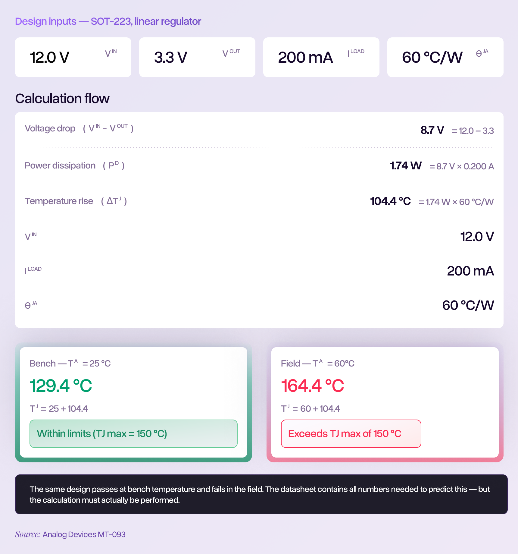
Consider a linear voltage regulator stepping 12V down to 3.3V at 200mA. The power dissipated is (12V - 3.3V) x 0.2A = 1.74W. In an SOT-223 package with a typical junction-to-ambient thermal resistance of 60 degrees C per watt, this produces a junction temperature rise of over 100 degrees C above ambient. At a 25 degrees C bench temperature, the junction reaches approximately 130 degrees C, within the typical 150 degrees C maximum. But in an enclosed industrial product operating at 60 degrees C ambient, the junction reaches approximately 165 degrees C — exceeding the absolute maximum and guaranteeing eventual failure.
Every number in that calculation is available in the relevant datasheets. Yet this calculation is frequently skipped, particularly for components that 'seem fine' because their rated current or power handling exceeds the load by a comfortable margin. The margin that matters is not the current margin or the power margin. It is the thermal margin, and that requires a calculation, not an assumption.
Building an interface specification matrix
The examples above — voltage thresholds, capacitor bias effects, thermal calculations — each represent a single category of specification that must be verified for a single component or interface. A moderately complex design might contain fifty to a hundred interfaces between active components, each requiring its own cross-referencing exercise.
This is where a specification matrix becomes not just helpful but essential. Rather than relying on mental tracking or ad hoc spot-checks, a matrix forces the engineer to explicitly document the critical parameters from both sides of every interface and evaluate compatibility in one place.
Consider a concrete example: a microcontroller UART connecting to a GPS module. The relevant specifications live in two datasheets, and the matrix reveals what must match:
Even this simplified matrix for a single two-wire interface surfaces several verification points that a quick visual review of the schematic might skip: the absolute maximum input voltage on the GPS module's RX pin, the need to cross-connect rather than wire TX-to-TX, and the pull-up configuration on both sides. For a design with fifty such interfaces, a matrix maintained in a spreadsheet and updated with each design revision imposes the systematic discipline that unstructured review cannot sustain.
Building the matrix is itself substantial work. But it transforms the verification task from an exercise in recall and vigilance into an exercise in documentation and completeness. The parameters that appear in the matrix get checked. The parameters that do not appear represent the residual risk — and making that risk visible is itself valuable.

The cross-referencing problem at scale
Each of the specification areas described above is individually manageable when an engineer focuses on a single interface. The challenge is that a moderately complex design might contain two hundred or more such verification points across all its interfaces, each requiring parameter extraction from different datasheets that organize information differently, use different terminology for equivalent concepts, and bury critical specifications in different locations.
As established in the first article of this series, complex inspection tasks produce miss rates of 20 to 30 percent even among experienced professionals. What that statistic means concretely in the context of datasheet cross-referencing is sobering: a design with 200 interfaces, each requiring verification of voltage levels, timing, current capability, and special pin requirements, is statistically expected to contain 40 to 60 connections where at least one critical parameter was not fully verified. Not because the engineer was careless, but because the task of sustained, accurate cross-referencing across that many documents and parameters exceeds what human attention reliably sustains under real project conditions.
A specification matrix helps. Derating discipline helps. Checking recommended operating conditions before absolute maximums helps. Consulting DC bias curves before finalizing capacitor selections helps. Performing junction temperature calculations for every component dissipating more than a few hundred milliwatts helps. These practices narrow the gap meaningfully. But they do not close it entirely, because they still depend on the engineer knowing which parameters to include and having the time to verify each one.
The specifications that get missed are often the ones the engineer did not know to look for: the bus capacitance that accumulated across six devices, the test condition footnote that changed the meaning of a threshold, the DC bias curve that was available but never consulted. No checklist eliminates these unknown unknowns completely. But formalizing the verification process — making it systematic and documented rather than implicit and ad hoc — converts a task that relies on vigilance into one that relies on process. That shift alone, even within the constraints of manual review, can meaningfully change how many specifications escape unverified into fabrication.

References
- 'Data Sheet Intricacies: Absolute Maximum Ratings and Thermal Resistances,' Analog Devices Technical Article. Notes that '90% of the problems/issues/failures that users face arise from careless or incorrect reading of the data sheet.'
- 'How to Read Power Supply IC Datasheets: Cover, Block Diagram, Absolute Maximum Ratings and Recommended Operating Conditions,' TechWeb (Rohm Semiconductor).
- 'Absolute Maximum Ratings,' Analog Devices, Rarely Asked Questions, RAQ Issue 50. Standard datasheet disclaimer.
- 'What is the difference between absolute maximum ratings and operating conditions?' Toshiba Electronic Devices and Storage Corporation.
- 'Selecting the Right Level-Translation Solution,' Texas Instruments Application Report SCLA049.
- 'A Brief Recap of Popular Logic Standards,' EE Times.
- 'Understanding the effect of DC bias on MLCC capacitance,' StarFish Medical. Documents a 4.7uF, 25V, X5R 0603 capacitor from Murata showing capacitance dropping to approximately 1.3uF at 10V.
- 'DC and AC Bias Dependence of MLCC Capacitors,' doEEEt.com.
- 'Capacitor Voltage Derating Guidelines for PCB Design,' Highleap Electronics, citing MIL-HDBK-338B, NASA Technical Standards, and IPC-9592B.
- 'How to Accurately Estimate IC Junction Temperature,' Analog Devices Technical Article.
- MT-093 Tutorial: 'Thermal Design Basics,' Analog Devices.
- 'The Art of Schematic Review: Catching Errors Before PCB Layout,' RunTime Recruitment.
- Drury, C.G. and Fox, J.G. (1975). Human reliability in quality control. Cited in 'The Role of Visual Inspection in the 21st Century,' U.S. Department of Energy, OSTI.